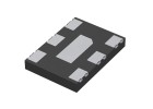
The CO75H4-20.000-33JDTSNK is a crystal oscillator (XO) module from Suzhou Hangjing Elec&Tech, designed to provide a precise 20.0000 MHz CMOS output in a standard surface-mount package. This component is a fixed-frequency oscillator, meaning it integrates a quartz crystal and an IC to generate a stable clock signal without requiring external tuning components. Its primary use is as a timing reference in digital systems, from microcontrollers to FPGAs and communication interfaces.
Starting with the key electrical specifications, the nominal frequency is 20.0000 MHz with a frequency stability that is typically specified in parts per million (ppm). For this SKU, the "33" in the part number often indicates a stability rating, likely ±33 ppm over the full operating temperature range. In practice, this means the actual output frequency can drift by up to 33 cycles per million from the nominal 20 MHz due to temperature changes. For a 20 MHz signal, this is a maximum deviation of about 660 Hz. This is critical for timing-sensitive applications like USB, Ethernet, or serial data links where even small jitter or frequency offset can cause data corruption. The "JDT" suffix may denote a specific temperature range, such as -40°C to +85°C, which is industrial grade. The supply voltage is 3.3V, indicated by the "33" prefix before "JDTSNK", which is standard for low-power CMOS logic. The current consumption, typically around 10-20 mA for a CMOS output at 20 MHz, should be verified from the datasheet. This is low enough for battery-powered devices but must be considered when calculating total system power.
Absolute maximum ratings are non-negotiable limits that, if exceeded, can permanently damage the oscillator. For this device, the supply voltage (Vdd) must not exceed the specified maximum, commonly 4.0V for a 3.3V rated part. Input voltage on any pin (usually only the enable/disable pin if present) should not exceed Vdd + 0.5V. Storage temperature is often -55°C to +125°C, but operating temperature is narrower. Derating is essential for reliability. If the system operates near the upper temperature limit, the oscillator's internal heating from self-heating (due to current draw) can raise the junction temperature further. A derating factor of 20-30% on the maximum operating temperature is wise for long-term reliability. Similarly, if the supply voltage is noisy or has transients, a decoupling capacitor (typically 0.1 µF ceramic) close to the Vdd pin is mandatory to prevent exceeding the absolute maximum voltage. Never apply reverse voltage or excessive mechanical stress to the package.
The typical application circuit is straightforward. The oscillator operates as a three-terminal device: Vdd, GND, and Output. The output is a CMOS square wave, capable of driving a standard logic input. The circuit should include a bypass capacitor of 0.1 µF placed as close as possible to the Vdd and GND pins to filter high-frequency noise. A bulk capacitor of 1-10 µF may be added on the power rail. The output is typically connected directly to the clock input of a microcontroller or FPGA. No external resistors are needed for the oscillator itself, but a series resistor of 22-33 ohms at the output can be used to reduce ringing if the trace is long. For applications with an enable/disable pin (common in XO modules), this pin must be tied to Vdd (or left floating if internally pulled high) to enable the output. If not used, it should not be grounded. The output load capacitance is standard for CMOS inputs, typically 15 pF, but the oscillator is designed to drive up to 15-30 pF. Excessive load capacitance will increase current and slow rise/fall times.
The pin configuration for this SMD package, likely a 4-pin or 6-pin ceramic or plastic package, is critical. Pin 1 is usually the enable/disable (E/D) or no connect (NC). Pin 2 is ground (GND), pin 3 is output (OUT), and pin 4 is supply voltage (Vdd). In a 6-pin variant, extra pins may be NC or GND. The package footprint is typically 5.0 x 3.2 mm or 7.0 x 5.0 mm, standard for oscillators. When soldering, ensure the pads align with the datasheet footprint to avoid short circuits. The component is sensitive to mechanical shock and should be handled with care during pick-and-place. Reflow soldering profiles must adhere to JEDEC standards, typically with a peak temperature of 260°C for lead-free solder. Avoid rapid cooling to prevent crystal damage.
Thermal management is generally not a concern for this low-power oscillator, but it must be considered in dense boards. The component can dissipate around 0.05W (20 mA at 3.3V). This heat is conducted through the GND and Vdd pins to the PCB copper. Ensure adequate copper area on these pins for heat sinking. In high-temperature environments, the internal crystal's aging and frequency stability may degrade. Using a thermal pad or via stitching under the GND pad can help. If the ambient temperature exceeds 85°C, consider a higher temperature rated variant. Do not place the oscillator near high-power components like voltage regulators or power transistors without proper spacing.
Interpreting timing diagrams and characteristic curves requires understanding the oscillator's behavior. The output waveform is a square wave with specified rise and fall times, typically a few nanoseconds. The timing diagram will show the output transitioning between 0V and Vdd (3.3V) with a duty cycle close to 50%. Key parameters are rise time (tr) and fall time (tf), measured between 10% and 90% of Vdd. For CMOS outputs, these are typically under 5 ns. The jitter, or short-term timing variation, is shown in a phase noise plot or as cycle-to-cycle jitter. This is critical for high-speed digital systems. The characteristic curves often include frequency vs. temperature plots, showing the ppm deviation over the temperature range. For a ±33 ppm oscillator, the curve will be a smooth parabola. Startup time is the time from power application to stable output, often 10 ms or less. The enable/disable timing shows how quickly the output turns on or off. Always check the test conditions in the datasheet, such as supply voltage and load capacitance, to ensure the curves match your application. Any deviation in load or supply will shift these parameters.

XTAL OSC XO 20.0000MHZ CMOS SMD
Suzhou Hangjing Elec&Tech Co.,Ltd | CO75H4-20.000-33JDTSNK | $1.30