Introduction to the Component and Why It Works for This Tutorial
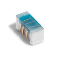
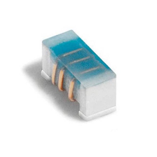
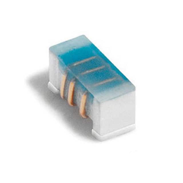
The Coilcraft 0402DC-43NXJRW is a fixed inductor with a nominal value of 43 nH, a current rating of 640 mA, and a DC resistance (DCR) of 430 milliohms. This component is ideal for a hands-on design tutorial because it sits in a sweet spot: it is small enough (0402 package) to challenge your soldering and layout skills, yet its moderate inductance and low DCR make it forgiving in prototyping. The 43 nH value is particularly useful for high-frequency filtering in the 100 MHz to 1 GHz range, such as in RF matching networks or decoupling circuits. Its self-resonant frequency (SRF) is typically above 2 GHz, so it behaves as a pure inductor in our target band. This tutorial will focus on designing a simple impedance-matching network for a 50-ohm system, a common real-world task.
Design Requirements and Specifications for a Practical Circuit
We will design a low-pass L-network to match a source impedance of 50 ohms to a load impedance of 100 ohms at a frequency of 433 MHz (a popular ISM band). The goal is to minimize insertion loss and ensure the inductor can handle the expected current. Key specifications: operating frequency = 433 MHz, source impedance = 50 ohms, load impedance = 100 ohms, maximum input power = +10 dBm (10 mW), which translates to about 14 mA RMS current through the inductor at 50 ohms—well below the 640 mA rating. The inductor’s Q factor at 433 MHz is approximately 45 (based on datasheet curves), which is acceptable for this design. We will use a series inductor-shunt capacitor topology for the L-network.
Step-by-Step Design Process with Calculations
First, determine the required reactance values. For an L-network matching 50 ohms to 100 ohms, the loaded Q is given by Q = sqrt((R_load/R_source) - 1) = sqrt((100/50) - 1) = 1. The series inductor reactance X_L = Q R_source = 1 50 = 50 ohms. The shunt capacitor reactance X_C = R_load / Q = 100 / 1 = 100 ohms. At 433 MHz, calculate inductance: L = X_L / (2πf) = 50 / (2π 433e6) ≈ 18.4 nH. Capacitance: C = 1 / (2πf X_C) = 1 / (2π 433e6 100) ≈ 3.68 pF. Our chosen inductor is 43 nH, not 18.4 nH. To use it, we must adjust the topology. Instead, we can design a high-pass L-network with a shunt inductor and series capacitor. For a 50-to-100 ohm match, the shunt inductor reactance X_L = R_source Q = 50 1 = 50 ohms, so L = 50 / (2π 433e6) ≈ 18.4 nH, still not 43 nH. Alternatively, we can use the inductor in a pi-network or as part of a resonant tank. For simplicity, let’s design a resonant impedance transformer: place the 43 nH inductor in parallel with a capacitor to resonate at 433 MHz. The resonant frequency formula: f_res = 1 / (2π√(LC)). Solve for C: C = 1 / ((2πf)^2 L) = 1 / ((2π433e6)^2 43e-9) ≈ 3.16 pF. This LC tank presents a high impedance at resonance. In series with a 50-ohm source, it can block DC while passing RF. We’ll use this as a DC-blocking and matching element. The current through the inductor at resonance is determined by the tank’s Q. With Q ≈ 45, the parallel resistance R_p = Q 2πfL = 45 2π 433e6 * 43e-9 ≈ 5,260 ohms, which is much higher than 50 ohms, ensuring minimal loading.
Component Selection Rationale for the Complete BOM
Beyond the Coilcraft 0402DC-43NXJRW inductor, we need: a 3.2 pF capacitor (standard value, use a 0402 C0G/NP0 ceramic for low loss), two SMA connectors for input/output, a 50-ohm microstrip test board (e.g., FR4 with εr=4.5, thickness 0.062”, trace width ~0.11”), and a few 0402 resistors for biasing if needed. The capacitor should have a Q > 200 at 433 MHz, easily met by C0G. For soldering, use a fine-tipped iron (300-350°C) and flux. The SMA connectors must be rated to 1 GHz. This BOM is minimal and focused on the critical inductor.
Simulation Tips and What to Look For
Use a free RF simulator like Qucs or LTspice. Model the inductor with its datasheet parameters: L=43 nH, DCR=0.43 ohms, and add a parallel capacitor of 0.2 pF to model parasitic capacitance (approximating SRF). Set up a 50-ohm source and 100-ohm load. Sweep frequency from 400 to 460 MHz. Look for the S11 (return loss) dip at 433 MHz—it should be below -15 dB for a good match. Also check S21 (insertion loss); expect about -0.3 dB due to DCR. If the dip is off-frequency, adjust the capacitor value slightly. The simulation should show the LC tank’s impedance peak at resonance. Note that the 3.2 pF capacitor may need trimming to account for PCB parasitics—simulate with 3.0 pF and 3.3 pF to see sensitivity.
Prototype Build and Testing Methodology
Fabricate a small PCB with a 50-ohm microstrip line. Solder the inductor and capacitor close to the connectors to minimize trace inductance. Use a vector network analyzer (VNA) calibrated with an SOLT kit. Connect the DUT (device under test) between port 1 and port 2. Measure S11 and S21 from 300 to 600 MHz. Initial results may show a resonant dip slightly off 433 MHz due to parasitic inductance in the capacitor or pad capacitance. Adjust the capacitor by adding a small parallel 0.5 pF or using a trimmer capacitor (1-5 pF) for fine-tuning. Ensure the inductor is not damaged by excessive heat during soldering (limit to 3 seconds per joint).
Performance Verification and Optimization
Verify the S11 is below -20 dB at 433 MHz, indicating a good impedance match. Check the insertion loss S21; if it exceeds -1 dB, the inductor’s DCR or the capacitor’s ESR is too high. Optimize by replacing the capacitor with a higher-Q C0G type or using a smaller package. If the resonant frequency shifts, recalculate the required capacitance using the measured inductor value (use a LCR meter at 1 MHz to confirm 43 nH). For production, consider the Coilcraft inductor’s tolerance (±5%) and temperature coefficient (typically ±25 ppm/°C). The final design should be stable from -40°C to +85°C. Document the measured results: resonant frequency, 3-dB bandwidth (should be around 10 MHz for Q=45), and maximum current handling (test with a signal generator at +10 dBm and confirm no saturation using a spectrum analyzer). This tutorial demonstrates how a specific inductor choice drives the entire design process, from calculations to real-world testing.